
- PRICING
- LIVE QUOTES
- LEARN
- HELP


EN
UBS: AI cloud demand accelerates the four main lines of comprehensive upstream semiconductor production expansion in Asia
The Zhitong Finance App learned that the UBS Asia Semiconductor team recently released the industry report “Asia Semis Pulse”, which shows four main lines of simultaneous acceleration: the TSM.US (TSM.US) A14 construction pace is ahead of schedule, MediaTek relies on Google (GOOGL.US) TPU (GOOGL.US) and the new ASIC project to open a second growth curve, silicon capacitors have become the new throat of AI packaging, and silicon wafers have entered the third upward cycle. The report's core judgment is that the demand for cloud AI is simultaneously pushing every aspect of the semiconductor upstream into a state of expansion — from 1.4 nanometer fabs to the most inconspicuous passive components.
A14 ahead of schedule: Baoshan's entry and Zhongke plant expansion were accelerated
According to UBS, TSMC is further accelerating the construction of its most advanced production capacity: the new node A14 will be the first to launch equipment in Baoshan Fab 20 in the second half of 2026, while plans to expand production originally scheduled for the Zhongke Fab 25 are being advanced to support a larger production capacity scale during mass production in 2028. UBS estimates that by the end of 2028, TSMC will have an A14 production capacity of about 60,000 pieces/month, which is higher than the N2 installed capacity of 30,000 to 40,000 pieces/month during the same period.
This judgment is mutually confirmed by public information about the supply chain in Taiwan, China. Taiwanese media reported on September 25 that the A14 has started trial production with the Hsinchu Baoshan Fab 20 and Zhongke Fab 25 to evaluate the viability of the nodes and allow customers to understand the performance of their designs in the mass production environment in advance. As the trial production progressed better than expected, the schedule was moved forward; according to the plan, the A14 will enter risky trial production in 2027 and mass production in Taiwan in 2028. Baoshan Fab 20's P3 plant has been licensed for the second quarter, and trial production is expected to begin in September, and trial production is expected in the first quarter of 2027; the P1 plant of Zhongke Fab 25, the main mass production area, is expected to be completed by April 2027, with P2 to P4 rushing up at the same time. The total A14 production capacity of the two plants is about 60,000 to 70,000 pieces/month.
In terms of specifications, compared to N2, the speed of A14 is increased by 10% to 15% at the same power consumption, or the power consumption is reduced by 25% to 30% at the same frequency, and the logic density is increased by more than 20%. Using second-generation nanosheet transistors and NanoFlex Pro standard units, the lithography still uses Low-NA EUV, and high-NA is not introduced until around 1 nm.
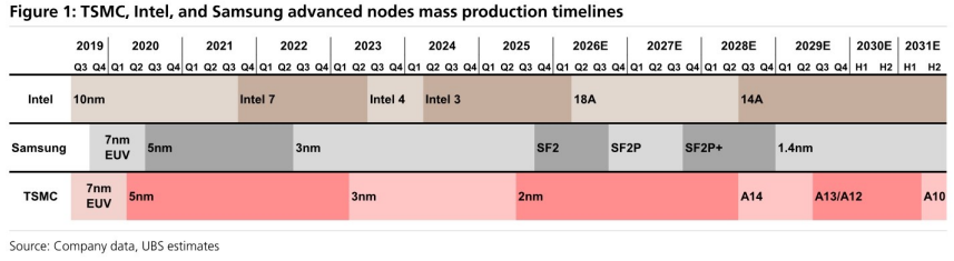
On the competitive side, UBS pointed out two contrasts: Intel (INTC.US) aims to mass produce 14A in 2028 and release PDK 1.0 later this year; Samsung Foundry's SF1.4 mass production seems to be delayed until 2029 due to yield challenges. Naga Chandrasekaran, head of foundry at Intel, publicly stated earlier that the performance gap between the 14A and TSMC A14 is expected to be within 5%, and plans to start risky trial production in the second half of 2027. In other words, from 2027 to 2028, the two companies will collide head-on in the Emmy era, leaving Samsung behind.
Capital expenditure increase: break $100 billion by 2028
Based on the larger expansion of N3 and N2 production and the faster A14 climb, UBS raised TSMC's capital expenditure forecast for 2027 and 2028 from 80 billion and 95 billion US dollars to 90 billion and 105 billion US dollars. This is the most direct numerical increase in this report.
On the production capacity side, the corporation estimates that TSMC's 2-nanometer monthly production capacity will reach 90,000 to 100,000 tablets by the end of this year and increase to 130,000 to 140,000 pieces in 2027. NANCO 3nm will have about 170,000 to 180,000 pieces in the fourth quarter of this year, and is expected to surpass 200,000 pieces next year — this means that 2027 will experience a rare situation where the three generations of N3, N2/A16, and A14 will simultaneously expand production and trial production. Digitimes, on the other hand, pointed out that TSMC's production capacity of 3 nm, 2 nm, and CoWoS advanced packaging continues to be in short supply. As Amazon AWS and MediaTek each increase their production plans due to large orders for self-developed AI chips and Google TPU, TSMC has readjusted its advanced production capacity allocation.
MediaTek: TPU v9 fixed, 20x in two years
The second main line of the report is MediaTek. UBS claims that the implementation of the EMIB-T packaging scheme for TPU v9 is turning positive: the substrate manufacturer Ibiden (Ibiden) improved yield, and Xinxing and Shinko Electric increased mass production support for TPU v9 below 2 nm; if demand for TPU v9 exceeds 4 million units in 2029, MediaTek is negotiating with TSMC to add CoWoS advanced packaging in addition to EMIB-T. It is reported that TPU v9 will use TSMC's CoWoS-L and Intel EMIB-T at the same time. TSMC has fine-tuned MediaTek's 3 nm and 2 nm production capacity arrangements after the front and rear supply models were changed.
The quantification part is more compelling. UBS estimates that Google's TPU sales will jump from $2.1 billion in 2026 to $18 billion in 2027, $43.5 billion in 2028, $52.5 billion in 2029, and $60 billion in 2030; in other words, 20 times in two years. The TPU business's share of MediaTek's revenue rose accordingly from 10% in 2026 to 65% in 2028 (68% and 69% in 2029 and 2030), while the TPU business's revenue contribution per share swelled from 8.1 NTD to 291.4 yuan in 2028 and 402 yuan in 2030.
What drives this estimate is a new project other than TPU. UBS says MediaTek is engaging with two new ASIC plans, which are expected to be finalized in recent months, with a total revenue opportunity of up to $10 billion to $15 billion: one is SpaceX's Dojo 3, which uses TSMC's 2 nm and wafer level system (SoW) package and may partner with Nvidia to provide NVLink Fusion; the second is Tesla AI6, which is intended to be manufactured first at Intel's fab and later transferred to Terafab.
On September 24, UBS published a separate MediaTek article: Reiterating the purchase, raising the target price from NT$6,500 to NT$7,300, and predicting MediaTek's 2027 revenue growth of 85% year-on-year to NT$1.25 trillion, and an increase of about 70% to 2.14 trillion yuan in 2028, with earnings per share of 363.36 yuan in 2028; UBS emphasized that its 2028 EPS estimate was 44% higher than market consensus. This pulsating report is an industry footnote to this judgment.
Silicon Capacitors: The New Throat for AI Packaging
The third main wire is a silicon capacitor. UBS's logic is that AI and HPC packages continue to grow in size, power consumption increases, power integrity becomes a key bottleneck, and silicon capacitors become a key component within the package. In the past, silicon capacitors basically only existed in TSMC's CoWoS and intermediary layer ecology, and will expand to the entire industry in the next few years as advanced packaging and testing plants such as Intel EMIB and Sun Moon Light expand to the entire industry; UBS estimates that the demand for silicon capacitors in non-TSMC systems may grow to 40,000 to 50,000 pieces per month by 2028 to 2029. Beneficiaries include LiSMC, which has already passed Intel's verification and begun shipping, and UMC, which joined in 2028 to 2029. Both companies have recently announced close cooperation with Apple Technology to expand the supply of silicon capacitors. Intel EMIB.
The extent to which supply and demand are tight has been quantified by various sources. The Morgan Stanley report estimates that as of June of this year, the global silicon capacitor shortage rate was as high as 57%, and there may be structural shortages for the next three years. The gaps in 2027 and 2028 are 16% and 11%, respectively. Production expansion on the industrial side is as intense as long-term: Samsung Electric announced a 1.557 trillion won (approximately US$1,035 million) long-term supply contract for silicon capacitors in May, with an execution period of January 2027 to December 2028, equivalent to 13.8% of its 2025 revenue; analog device giant ADI bought silicon capacitor manufacturer Empower Semiconductor for $1.5 billion and completed delivery in July. These components must be introduced at the package design stage, and they also have to go through at least two years of reliability verification. Once certified, the company plans to increase the monthly production capacity of 12-inch silicon capacitors by three to four times in the second half of 2027; UMC claims that the advanced packaging business already has more than ten customers and will expand to more than 35 new designs next year.
The demand-side certainty comes from two AI leaders: Nvidia's Rubin architecture has included embedded silicon capacitors as standard, and Intel plans to begin large-scale adoption of silicon capacitors in 2027 to enhance EMIB performance. Aipu Technology's performance has proven a trend — consolidated revenue for the second quarter of 2026 was NT$2.36 billion, an annual increase of 78%. Among them, stacked silicon capacitors (s-SiCAP) contributed 640 million yuan, an annual increase of 273%, accounting for 27% of revenue.
However, Businessweek also suggested a ceiling: Compared with mature manufacturing processes of 28 nanometers or more and an annual output value of more than 70 billion US dollars, the global output value of silicon capacitors this year is only about 2.3 billion US dollars, which is not enough to change the capacity allocation and profit structure; if silicon capacitors can never be attached to AI chips, their upper limit will be locked by advanced packaging production capacity.
Silicon wafers: third upward cycle
The fourth main line is a silicon wafer. UBS quoted Taiwanese media reports as saying that Hejing is negotiating with customers on a new round of price increases of about 8%; if confirmed, this will be its second round after increasing some 6-inch and 8-inch customers by about 10% in the second quarter (effective in the second half of 2026). According to UBS's judgment, if new production capacity is to be implemented, a meaningful price increase is necessary to resolve supply constraints by 2028. The price increase began in the first half of 2026, and the year-on-year increase from 2027 to 2028 may exceed 20%; the report compared the 12-inch wafer utilization rate with Global Crystal's price, pointing out that this is the third round of the upward cycle following 2017 to 2018 and 2021 to 2022.
The verification of the industrial chain is also intensive. In May of this year, Shin-Etsu Chemical, SUMCO and Global Crystal simultaneously issued a letter of price increase, starting the second round of price adjustments during the year. 12-inch conventional products increased by 5% to 8%, and high-grade special silicon wafers for AI and HPC increased by 18% to 22%; entering the second half of the year, 6-inch, 8-inch, and 12-inch full-size price increases for the first time in more than three years, starting at 10%. The price increase of about 10% was completed in the first half of the year and implemented in the second half of the year. The company confirmed that it is negotiating quotations for other 8-inch customers. The new price may be applied from 2027, and the 12-inch price has not been adjusted; Xu Xiulan, chairman of Global Crystal, bluntly stated that both spot and long-term contract prices have entered an upward channel.
The demand-side figures come from SUMCO's estimates: AI servers demand 12-inch silicon wafers 3.8 times that of general-purpose servers, and HBM consumes 3 times that of mainstream DRAM at the same capacity. Monthly demand for AI-related advanced process silicon wafers is expected to exceed 1 million wafers in 2026, accounting for more than 10% of the world's total 12-inch demand. According to SEMI data, global silicon wafer shipments in the second quarter of 2026 increased 7.4% year on year and 9.1% month on month to reach 3,573 million square inches, a record high in a single quarter of nearly two years, and has been growing positively for four consecutive quarters (SEMI, SUMCO).
conclusions
Looking at these four lines together, UBS's pulsating report actually gave a judgment: the bottleneck in AI computing power is spreading from “computing power chips” to “every supporting link” — advanced processes need to be put into production in advance, packaging needs to be prepared in advance, and prices for upstream silicon wafers need to rise early. The report also provides two variables to track: one is whether TSMC's capital expenditure of US$105 billion in 2028 can be realized as actual production capacity, and the other is MediaTek's choice of packaging route between CoWOS and EMIB-T, which will determine whether it can eat TPU demand after 2029.