
- PRICING
- LIVE QUOTES
- LEARN
- HELP


EN
CINNO Research: Investment in China's semiconductor industry reached 802 billion yuan in the first half of the year, a year-on-year increase of 72.4%
Zhitong Finance App learned that CINNO Research chief analyst Zhou Hua Charley said that according to the latest statistics from CINNO • IC Research, the total investment in the semiconductor industry in China (including Taiwan) reached 800.2 billion yuan in the first half of 2026, an increase of 72.4% over the previous year, and the scale of investment expanded dramatically. As a result, there was a clear divergence between the growth rate of investment in segmented tracks and the share of capital, and there was a fundamental shift in investment focus from previous years.
1. The overall investment pattern of China's semiconductor industry in the first half of 2026: the total amount rose sharply, and the capital structure was simultaneously restructured according to demand and regulation
According to the latest statistics from CINNO • IC Research, the total investment in the semiconductor industry in China (including Taiwan) reached 800.2 billion yuan in the first half of 2026, an increase of 72.4% over the previous year, and the scale of investment expanded significantly. This rapid growth reflects the concentrated release of demand for terminals such as AI computing power and automotive-grade chips. At the same time, in the context of deep adjustments in the global supply chain pattern, industrial capital is actively strategically allocating towards high barriers in the industrial chain. Judging from the driving logic, investment drivers in different regions are clearly divided due to differences in the industrial base and external environment: mature market investment is more driven by global customer orders and market demand, while mainland China is increasingly concentrated on equipment, materials, and advanced packaging under the dual effects of supply chain autonomy and changes in the external environment. As a result, there was a clear divergence between the growth rate of investment in segmented tracks and the share of capital, and there was a fundamental shift in investment focus from previous years.
Investment data for each track segment in the first half of 2026 is deeply tied to industry changes. Compared with the investment logic of balanced production expansion in previous years, it no longer simply pursues scale expansion on the manufacturing side. Relying on structural differences in investment amounts and growth rates of each track, it guides capital to focus on high-growth advanced packaging and semiconductor materials with domestic alternative space, while maintaining the expansion of characteristic wafer processes and continuous investment in equipment R&D. It relies on investment structure optimization to hedge external industry pressure and save momentum for technological breakthroughs.
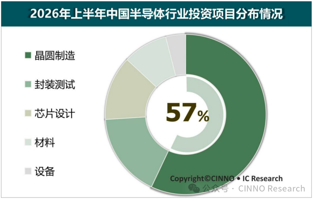
Illustration: Distribution of investment projects in the semiconductor industry in China (including Taiwan) in the first half of 2026. Source: CINNO • IC Research
Wafer manufacturing invested 452.7 billion yuan, accounting for 56.6% of the total investment of the entire industry. The year-on-year growth rate was 93.4%, which was higher than the industry average. Although production capacity of mature traditional consumer electronics processes is becoming saturated, and related production expansion projects have declined markedly, production lines with AI memory chips and vehicle power characteristics have been concentrated, driving the manufacturing sector to continue to lead the entire industry chain in terms of investment volume, and more than half of the capital is still concentrated on the manufacturing side;
Investment in semiconductor materials was 74.90 billion yuan, accounting for 9.4% of the total investment, up 38.9% year on year. The growth rate improved rapidly. Capital allocation was skewed towards high-end categories, and investment in high value-added materials increased significantly compared to previous years;
Investment in chip design was 107.3 billion yuan, accounting for 13.4% of the total investment, up 18.4% year on year. The growth rate was steady and upward. Industry capital faded away from the trend of blind expansion, capital was concentrated in high barrier segments such as computing power and vehicle regulations, and investment in low-end consumer chips cooled down sharply;
Packaging testing invested 137.3 billion yuan, accounting for 17.2% of the total investment, up 225.5% from the previous year. It is the leading growth fault sector among all racetracks. Production capacity for advanced packaging such as HBM and 3D stacking is scarce, driving a large-scale influx of capital, and the share of capital has increased several times compared to previous years;
Investment in semiconductor equipment was 28.20 billion yuan, down 35.0% year on year, making it the only investment contraction circuit; the core reason was that export controls between the US, Japan and the Netherlands continued to upgrade, overseas equipment imports were blocked, and the short-term investment scale naturally declined, and equipment procurement has now entered the digestion period; the strategic position of the racetrack has not weakened; leading companies bucked the trend and expanded production, industrial mergers and acquisitions accelerated, and capital was shifting from “casting a wide net” to “betting on headlines+ mergers and acquisitions”.
2. Hefei Changxin's IPO leads the wave of domestic storage investment, and the main chain effect drives capital resonance throughout the industry chain
Changxin Technology, a leading domestic DRAM storage company, officially landed on the Science and Technology Innovation Board in the first half of 2026, becoming a key event throughout the investment logic of various circuit segments. This IPO raised an initial capital of 29.50 billion yuan, making it the largest A-share IPO in 2026 and the second largest IPO in the history of the Science and Technology Innovation Board. It was only 148 days from acceptance to completion, setting a new record for the review speed of large semiconductor companies on the Science and Technology Innovation Board.
29.5 billion yuan was raised and all invested in the main business: 7.5 billion yuan to upgrade and expand production of 12-inch wafer production lines, 13 billion yuan to iterate advanced DRAM processes such as 17nm DDR5 and LPDDR5X, and 9 billion yuan to develop forward-looking technologies such as HBM and 3D stacked DRAM.
Changxin Technology's main chain effect is not limited to its own investment, but also drives upstream and downstream collaborative production expansion through multi-dimensional linkages such as equipment procurement, material introduction, sealing and testing support, and technical collaboration. Of the capital raised, about 22.0 billion yuan was directly used for equipment procurement, providing reliable order support for local equipment leaders such as Huachuang and Tuojing Technology in the North. At the same time, the process iterated from 19nm to 17nm, directly driving an increase in the share of investment in 12-inch storage-grade silicon wafers and high-end electronic chemicals; the forward-looking layout of HBM and 3D stacked DRAM also formed technical collaboration with the explosive growth of sealed testing tracks, driving the demand for advanced downstream sealing and testing. The investment expansion of chain-leading enterprises, transmitted through a multi-dimensional industrial chain, is one of the core drivers of total investment scale expansion and structural restructuring in the first half of 2026.
3. Investment regions are highly concentrated in the Yangtze River Delta, and material circuit capital is fully concentrated on core consumables
Geographical distribution: The top five mainland regions attracted 77.2% investment, and the Yangtze River Delta industrial cluster effect continues to strengthen
According to the latest statistics from CINNO • IC Research, the degree of geographical differentiation of semiconductor investment in mainland China continued to increase in the first half of 2026 as the scale of capital increased, with the top five regions concentrating more than 70.0% of domestic industrial capital. Anhui ranked first with 46.10 billion yuan, accounting for 19.1% of the mainland's total investment; Jiangsu invested 44.59 billion yuan, accounting for 18.5% of total investment; Jiangsu invested 44.59 billion yuan, accounting for 18.5%, and the complete wafer manufacturing and testing supporting industry chain continued to attract capital; Shanghai accounted for 17.5% of the investment, focusing on high-end R&D; Guangdong and Zhejiang ranked fourth and fifth with 11.7% and 10.5% capital respectively.
The core driving force behind the stratification of investment amounts in various regions is the upstream and downstream supporting cost advantages brought about by the complete industrial chain in the Yangtze River Delta, and the differentiated industrial policies of each region to guide targeted capital accumulation. After the regional collaborative division of labor was formed, repeated construction and diversion investment was avoided, and the leading regions continued to absorb new projects, further boosting the capital accumulation ratio.
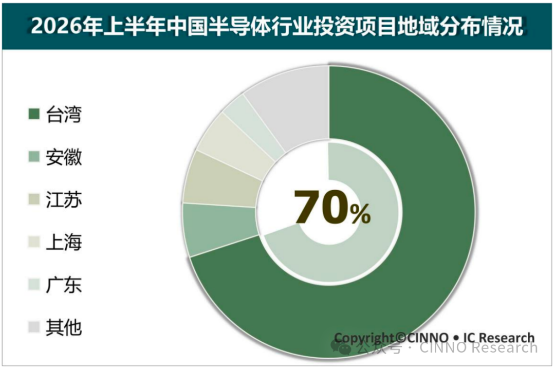
Figure: Geographical distribution of semiconductor industry investment projects in China (including Taiwan) in the first half of 2026. Source: CINNO • IC Research
Material circuit: capital is fully concentrated on core consumables, and the investment logic shifts from “expanding production volume” to “improving quality”
According to the latest statistics from CINNO • IC Research, capital allocation in 2026 is clearly skewed towards high-tech barrier categories such as electronic chemicals and electronic specialty gases. The usage and value of products such as photoresists and wet electronic chemicals in the 12-inch advanced manufacturing process increased simultaneously, driving the growth rate of investment in this segment to outperform the overall growth rate of the materials sector. The high concentration of core material categories goes hand in hand with a high growth rate, reflecting a deep shift in the investment logic in the materials sector from “expanding production volume” to “improving quality”.
The entire silicon industry chain invested a total of 34.64 billion yuan, of which 19.24 billion yuan was invested in silicon substrates (finished silicon wafers), focusing on 12-inch automotive-grade and storage-grade silicon wafers; upstream electronic grade silicon materials and single crystal rods totaled 15.40 billion yuan to expand production of raw materials supporting silicon wafers. Electronic chemicals invested 7.63 billion yuan, accounting for 11.2%; electronic specialty gas invested 6.06 billion yuan, accounting for 8.9%. Together, the three core materials account for more than 60% of the investment share in the materials sector, and capital is highly concentrated on the most rigid and continuously consumed link in the industrial chain.
Looking forward to the future, the industry has entered the “intensive cultivation” stage. Judging from endogenous variables, subsequent investment trends will depend on the ability of high-growth racetracks such as advanced packaging and core materials to accept incremental capital, as well as the continuous optimization of capital allocation by industrial policies. Looking at the global industrial landscape, overseas capital focuses on advanced manufacturing processes and AI support, while domestic capital relies on high total investment to break out of the independent market, and the precise guidance of large funds forms a synergy with the market-based drive of chain owners. China's semiconductor industry is moving from a “policy support period” to a “performance delivery period”, forming a positive cycle of production capacity release and investment expansion.