
- PRICING
- LIVE QUOTES
- LEARN
- HELP


EN
Wedbush: MediaTek EMIB yield review “fully confirms” Google TPU to Intel (INTC.US) package
The Zhitong Finance App learned that Intel (INTC.US)'s advanced packaging technology is at a critical turning point. MediaTek (MediaTek) made it clear at last week's legal conference that the yield rate of Intel's EMIB (Embedded Multi-Chip Interconnect Bridging) advanced packaging technology “has reached a very good level.” The statement quickly drew a lot of attention from Wall Street — Wedbush analysts pointed out that MediaTek's comments “further validate Intel's progress in packaging” and may mean that Google's (GOOGL.US) TPU order is within easy reach.
MediaTek “Official Announcement”: Yield standards met, second-generation ASIC mass production on time in 2028
MediaTek CEO Cai Lixing gave the clearest positive review so far on the progress of Intel's EMIB-T packaging technology at the legal conference last week. He said that back-end packaging technology is a key part of the entire complex ASIC, and the cooperation between MediaTek and suppliers has gone deep into operational details such as carrier board yield improvement, capacity supply, and production cycle time, “item-by-item management.”
Cai Lixing admits that EMIB is making good progress in yield improvement and technical maturity, enough to catch up with the 2028 mass production schedule. MediaTek Finance Director Gu Dawei stated more directly in response to the question “whether TSMC CoWos production capacity needs to be reserved for the second-generation project” — judging from all the positive data and results obtained so far from the second project, MediaTek is confident that mass production tasks will be completed as scheduled, and the current EMIB route no longer requires filing.
According to supply chain information, the post-production yield of Intel's EMIB-T package has broken through 90%, reaching the mass production threshold, and is expected to be officially mass-produced in 2026. In terms of cost, EMIB-T replaced the expensive large-area silicon intermediate layer with a small-area silicon bridge, and the packaging cost was reduced by more than 40% compared to TSMC's CoWoS solution.
Wedbush: MediaTek review “fully confirms” Google's TPU transfer speculation
Wedbush analyst Matt Bryson pointed out in the latest report that MediaTek's statement on EMIB yield has multiple meanings.
First, the speculation that Google TPU uses EMIB has been “fully confirmed.” Earlier, it was rumored in the market that Google's next TPU would abandon TSMC's CoWOS and switch to Intel's EMIB-T package. As the core ASIC design partner of Google TPU, MediaTek's positive evaluation of EMIB yield directly verified the viability of this technology path.
Second, the collaboration between MediaTek and Google is heating up. Bryson pointed out that MediaTek management raised the 2027 AI ASIC market share target from 10%-15% to 15%-20% at the French conference last week. Based on the 2027 serviceable market (SAM) of $80 billion, the corresponding potential revenue could reach $12 billion to $16 billion. The first AI ASIC is expected to be mass-produced in the fourth quarter of 2026, with a confirmed revenue contribution of 2 billion US dollars.
Intel's “double breakthrough” in the packaging business
MediaTek's endorsement was not an isolated incident. Intel is simultaneously ushering in both technical and commercial breakthroughs in the field of packaging:
At the technical level, EMIB-T is Intel's next-generation 2.5D advanced packaging technology and is positioned as a low-cost alternative to TSMC CoWoS. Vertical power supply is achieved through silicon holes, expensive intermediate layers are removed, costs are greatly reduced, and silicon wafer utilization is increased. Intel claims it can reach 8 to 10 times the size of the light mask complex by 2026.
On a commercial level, Intel Foundry Industry (IFS) just announced last month that cybersecurity giant Feita Information (FTNT.US) has become its first publicly named external OEM customer. If the Google TPU package order is placed, it will become IFS's most powerful external customer cooperation so far.
J.P. Morgan believes that the cooperation between Intel and Google should be limited to the packaging business rather than foundry - TPU will still be OEM by TSMC, and Intel will only be responsible for packaging. Even so, this is still a major breakthrough for Intel — advanced packaging is one of the fastest growing parts of AI chip manufacturing, and TSMC's CoVos production capacity has been in short supply for a long time.
MediaTek's AI ASIC blueprint: from $2 billion to $16 billion
MediaTek's AI ASIC business is showing an explosive growth trajectory:
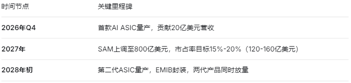
MediaTek also uses TSMC's CoWOS and Intel EmiB-T dual-package strategies to meet the large-scale AI chip design needs of different customers. Cai Lixing emphasized that the “performance per TCO” and “performance per watt” of second-generation ASICs will be greatly improved. Citibank is more optimistic that its relevant revenue in 2027 could reach $18 billion.
Conclusions
MediaTek's positive evaluation of EMIB yield enabled Intel's technology route in the field of advanced packaging to receive the highest level of endorsement from core partners. Wedbush believes this “fully confirms” speculation that Google's TPU will use Intel EMIB.
For Intel, if Google's TPU packaging order is officially implemented, it will be a major victory for its IDM 2.0 transformation strategy — proving that it can not only win external customers (Fortinet) in the field of wafer manufacturing, but also compete head-on with TSMC in the fastest-growing advanced packaging sector. As far as MediaTek is concerned, the AI ASIC revenue growth curve from 2 billion US dollars to 16 billion US dollars is being reshaped from the “king of mobile phone chips” to “an important player in AI chips.”