


Are “AI deceleration” concerns noise? ASML.US (ASML.US), the upstream chip “weather vane”, sends an optimistic signal: demand is booming, and the boom has not come to an end yet!
The Zhitong Finance App learned that when Dutch chip equipment manufacturer ASML.US (ASML.US) broke ground for a new plant in Eindhoven last week, Chief Financial Officer Roger Dassen (Roger Dassen) said that the AI boom has completely changed customer sentiment. The company's current $200 million EUV lithography machine — a key device for manufacturing advanced AI chips — has almost sold out of production capacity until 2027, while customers have made successive promises to use its next generation of $400 million High NA devices.
“Can you give me some more? Can you give it to me soon?” ——This is the tone of Darson's description of a recent conversation with a major customer.
TSMC, Samsung, and SK Hynix have all set a schedule to begin using High NA in mass production, and early adopter Intel said these machines have met production capacity and reliability standards. Coupled with new production expansion plans, these developments suggest that the European company by market capitalization is expected to continue its dominance in chip lithography until the 2030s.
“To be honest, I don't think we've reached the end of [the AI boom],” CEO Christophe Fouquet said over the phone.
From “questioning pricing” to “collective promises”, AI chip demand prospects are still strong
Asmack's customers include all major chip manufacturers, the most notable of which is TSMC, which manufactures chips for Apple and Nvidia. TSMC has previously questioned whether High NA is worth the money—around $400 million per device—but has now promised to adopt the technology starting in 2030.
Over the years, chip makers have been evaluating whether advances in manufacturing technology such as chip packaging and 3D stacking can reduce the demand for High NA. Today, these promises show that the biggest players in the industry still expect that reducing the size of chip features is still the only way to improve performance.
High NA can print approximately 40% smaller in characteristic size than standard EUV systems, and is expected to cut manufacturing steps and improve production efficiency — but the cost is about twice that of the former.
The industry is aligned around new tools
The trillion-dollar global semiconductor industry often makes investment decisions several years ahead of chip mass production. Manufacturers, equipment suppliers, and material companies need to coordinate to ensure that new equipment, chemicals, and processes can work together. Experts have previously questioned whether chipmakers will adopt High NA widely enough to recoup their R&D costs.
“I never doubted it because there was no other choice,” said InsingerGilissen analyst Jos Versteegh (Jos Versteegh).
Samsung said it will begin memory chip production with High NA devices in 2028, and Morningstar's Coreonero said this schedule was earlier than market expectations. Storage expert SK Hynix also announced that it will use High NA from 2028; Micron has ordered the device, but no date has been set for production. Intel — the first adopter of the technology — said on Tuesday (September 8) that it has processed more than 1 million wafers with High NA tools.
Fukai said that due to the smaller size of the finished chips from storage manufacturers, they have a lower threshold for using High NA.” “You'll see that these vendors are more aggressive in their plans on many things, and High NA is in it,” he said. “All of them are moving forward with plans to introduce High NA into mass production.”
A Bigger “Canvas”: The 12" Mask Initiative
According to reports and Asmack's official announcement, another more far-reaching industry initiative was revealed at the same time as the schedule: promoting the transition from the 6-inch photomask standard that has been in use for decades to 12 inches. The maximum exposure area of a single chip in existing EUV devices is about 800 square millimeters. Large data center chip designs from companies such as Nvidia and Google are approaching this upper limit; however, the exposure area of High NA is limited due to the use of smaller masks. By expanding the mask size, the next generation of devices will be able to produce products comparable to today's largest data center chips.
“If we can do it as an industry, you'll see the productivity of these devices increase by 40%,” said Marco Pieters (Marco Pieters), chief technology officer at Asmack. The initiative plans to build a pilot line by 2031 and be ready for mass production by 2033; for AI accelerators and GPUs that are growing in size, this transition will also avoid yield risks associated with the splicing process.
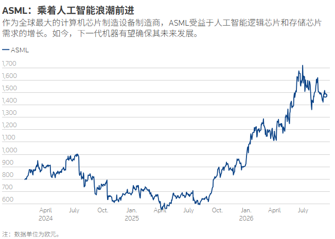
In terms of institutional perspective, Bank of America analyst Didier Semama reiterated Asmack's “buy” rating. He wrote in the report that these announcements are consistent with his predictions for the pace of High NA adoption (5 units this year, 6 units next year, 20 units by 2030). “Although these orders have not changed our financial forecasts, they have significantly strengthened the market's confidence that the industry chain is progressing collaboratively around a unified High NA roadmap.” According to another report, Barclays assessed that the promises of the three major customers provided clearer adoption visibility, and “demand is clearly strong”; Asmack's stock price has risen about 120% in the past year, and plans to expand EUV production capacity by about 30% in 2027.
Monopoly power: the indicative effect of Asmat signals on the market
J.P. Morgan estimates that Asmack will account for 94% of the global lithography market in 2025. At the cutting edge, its position is even more stable: Since the late 2010s, Asmat has had a monopoly on extreme ultraviolet (EUV) lithographs — the equipment necessary to make the smallest circuits in the most powerful commercial AI chips. First shipped in 2023, High NA is the next generation of EUV technology.
In the EUV field, Asmack has no commercial competitors. Deep ultraviolet (DUV) lithography systems manufactured by Japan's Nikon, Canon, and emerging Chinese competitors are older generation technology. Morningstar (Morningstar) analyst Javier Coreonello said that he is worried that these companies will soon catch up with Asmack in the field of lithography is tantamount to “misinformation.”
Technical depth: 35% increase in throughput, 93% availability target
The commercialization progress of High NA EUV is supported by substantial data. Greet Storms, senior vice president of Asmack, revealed that as of mid-July 2026, the cumulative number of exposed wafers in the global High NA EUV system had exceeded 1.35 million; the certified EXE:5200B system reached a throughput of 135 wafers per hour during acceptance tests, an increase of 35% over 100 wafers per hour of the previous generation EXE:5000.
Equipment stability is also improving. The global High NA fleet availability rate has increased to 84% from the level at the beginning of the year. ASML expects to reach 90% in the fourth quarter of 2026, with a medium- to long-term target of 93%.
Intel has mass-produced some Core Ultra Series 3 processors codenamed Panther Lake using High NA on the 18A process node. The production line in Oregon has completed dual certification, and the yield has reached the same level as the existing NXE platform. Fukai commented, “Some of the products you bought from Intel today were made with High NA equipment. This is a very important milestone. ”
The order-side data was also shocking. Asmat revealed in July that it has almost all the EUV equipment orders it needs in 2027 and has already received a large number of 2028 EUV forward orders. The company plans to increase the production capacity of low-NA EUV and submersible DUV equipment by 30% for two consecutive years in 2027 and 2028. Revenue guidance for the full year 2026 has been raised to 43 billion to 45 billion euros, a significant increase from previous expectations.
Insingergilissen analyst Jos Versteeg's comment went straight to the point: “I never doubted that High NA would be adopted because there were no alternatives. ”
Market Background: Three AI Leaders Call for “Slowing Down”
As the market digests High NA's long-term roadmap, a controversy over AI security erupted over the weekend.
According to reports, on September 12 (Saturday) local time, Anthropic CEO Dario Amodei said that the company will introduce more safeguards, including independent third-party evaluations, and urged the entire industry to slow down the development of the most advanced models. OpenAI CEO Sam Ultrman supported this, while xAI's Elon Musk responded “Dario was right.”
This rare consensus among the heads of the AI Big Three has become a new trigger for chip stocks. In the dark market trading on the evening of September 13, Beijing time, chip stocks collectively dived: SK Hynix and Intel fell 4%, Micron Technology, AMD, and SanDisk fell 3%, and Nvidia fell 2%. Market analysts pointed out that the slowdown in AI development may put pressure on chip makers and supply chain stock prices in the short term, but given that computing infrastructure spending is still strong, the long-term impact may be limited.
Gary Tan, portfolio manager at Allspring Global Investments in Singapore, said: “This may cause some short-term pressure, but it is unlikely to disrupt long-term AI transactions. AI development is still relatively early, and I'm not sure if other players in the AI ecosystem are willing to accept the current industry rankings and slow down while technology is still evolving so fast.”
Notably, this security dispute is a delicate trade-off with Asmack's long-term roadmap: AI leaders are calling for caution, and chipmakers are writing capacity competition promises beyond 2030. Also, according to a Reuters report, Anthropic is in talks to introduce Nvidia as a cornerstone investor. It plans to raise up to 100 billion US dollars, with a valuation of 2 trillion US dollars, which is expected to become the largest IPO in history — the giants' long-term bets on AI infrastructure have not cooled down due to a war of words.
The “Full Speed Operation” of the Capital Machine: The Gap Between Verbal Slowdown and Actual Acceleration
However, when executives publicly talked about “deceleration,” the pace of investment at the industrial level did not slow down.
The Bank for International Settlements previously warned that the five largest global cloud computing companies are expected to invest more than 1 trillion US dollars in AI from 2025 to 2026, and are increasingly dependent on debt financing. OpenAI expects its computing power spending to reach about 750 billion US dollars by 2030, up more than 25% from the previous forecast of about 600 billion US dollars. Oracle's capital expenditure for the first quarter reached US$28.5 billion, exceeding total revenue for the quarter. The capital expenditure of the four major US CSPs increased 86% year-on-year in the second quarter, and TrendForce has raised the capital expenditure estimates of the nine major cloud vendors for the whole year to 886.7 billion US dollars.
This “discrepancy between words and actions” is not simply a discrepancy in appearance; it is a structural dilemma facing the AI industry: no laboratory is willing to bear the cost of slowing down alone. As Axios reports, more and more people in the AI industry are admitting that the pace of development of technological capabilities may need to slow down, but “no single lab is willing to bear the cost of slowing down alone.”